 The year of 2013 was also a boon for the high-tech industry, especially where electronics and additive manufacturing were concerned. In fact, several key developments took place last year that may help scientists and researchers to move beyond Moore’s Law, as well as ring in a new era of manufacturing and production.
In terms of computing, developers have long feared that Moore’s Law – which states that the number of transistors on integrated circuits doubles approximately every two years – could be reaching a bottleneck. While the law (really it’s more of an observation) has certainly held true for the past forty years, it has been understood for some time that the use of silicon and copper wiring would eventually impose limits.
 Basically, one can only miniaturize circuits made from these materials so much before resistance occurs and they are too fragile to be effective. Because of this, researchers have been looking for replacement materials to substitute the silicon that makes up the 1 billion transistors, and the one hundred or so kilometers of copper wire, that currently make up an integrated circuit.
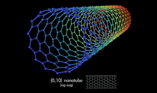
Various materials have been proposed, such as graphene, carbyne, and even carbon nanotubes. But now, a group of researchers from Stanford University and the SLAC National Accelerator Laboratory in California are proposing another material. It’s known as Stanene, a theorized material fabricated from a single layer of tin atoms that is theoretically extremely efficient, even at high temperatures.
 Compared to graphene, which is stupendously conductive, the researchers at Stanford and the SLAC claim that stanene should be a topological insulator. Topological insulators, due to their arrangement of electrons/nuclei, are insulators on their interior, but conductive along their edge and/or surface. Being only a single atom in thickness along its edges, this topological insulator can conduct electricity with 100% efficiency.
The Stanford and SLAC researchers also say that stanene would not only have 100%-efficiency edges at room temperature, but with a bit of fluorine, would also have 100% efficiency at temperatures of up to 100 degrees Celsius (212 Fahrenheit). This is very important if stanene is ever to be used in computer chips, which have operational temps of between 40 and 90 C (104 and 194 F).
Though the claim of perfect efficiency seems outlandish to some, others admit that near-perfect efficiency is possible. And while no stanene has been fabricated yet, it is unlikely that it would be hard to fashion some on a small scale, as the technology currently exists. However, it will likely be a very, very long time until stanene is used in the production of computer chips.
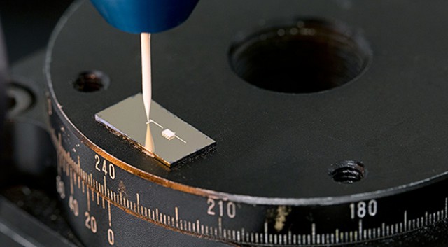 In the realm of additive manufacturing (aka. 3-D printing) several major developments were made during the year 0f 2013. This one came from Harvard University, where a materials scientist named Jennifer Lewis Lewis – using currently technology – has developed new “inks” that can be used to print batteries and other electronic components.
3-D printing is already at work in the field of consumer electronics with casings and some smaller components being made on industrial 3D printers. However, the need for traditionally produced circuit boards and batteries limits the usefulness of 3D printing. If the work being done by Lewis proves fruitful, it could make fabrication of a finished product considerably faster and easier.
 The Harvard team is calling the material “ink,” but in fact, it’s a suspension of nanoparticles in a dense liquid medium. In the case of the battery printing ink, the team starts with a vial of deionized water and ethylene glycol and adds nanoparticles of lithium titanium oxide. The mixture is homogenized, then centrifuged to separate out any larger particles, and the battery ink is formed.
This process is possible because of the unique properties of the nanoparticle suspension. It is mostly solid as it sits in the printer ready to be applied, then begins to flow like liquid when pressure is increased. Once it leaves the custom printer nozzle, it returns to a solid state. From this, Lewis’ team was able to lay down multiple layers of this ink with extreme precision at 100-nanometer accuracy.
 The tiny batteries being printed are about 1mm square, and could pack even higher energy density than conventional cells thanks to the intricate constructions. This approach is much more realistic than other metal printing technologies because it happens at room temperature, no need for microwaves, lasers or high-temperatures at all.
More importantly, it works with existing industrial 3D printers that were built to work with plastics. Because of this, battery production can be done cheaply using printers that cost on the order of a few hundred dollars, and not industrial-sized ones that can cost upwards of $1 million.
Smaller computers, and smaller, more efficient batteries. It seems that miniaturization, which some feared would be plateauing this decade, is safe for the foreseeable future! So I guess we can keep counting on our electronics getting smaller, harder to use, and easier to lose for the next few years. Yay for us!
Sources: extremetech.com, (2)