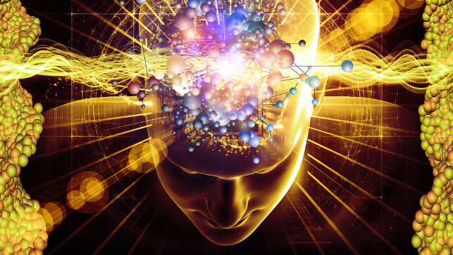
It’s no secret that computer scientists and engineers are looking to the human brain as means of achieving the next great leap in computer evolution. Already, machines are being developed that rely on machine blood, can continue working despite being damaged, and recognize images and speech. And soon, a computer chip that is capable of learning from its mistakes will also be available.
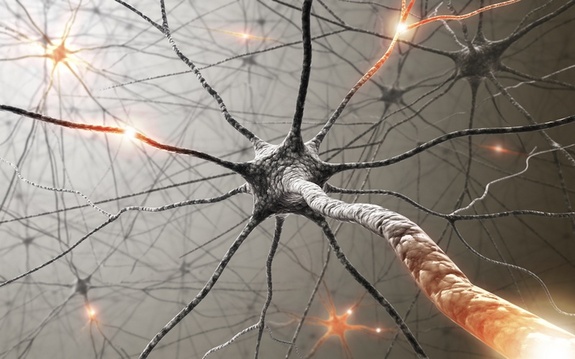
The new computing approach, already in use by some large technology companies, is based on the biological nervous system – specifically on how neurons react to stimuli and connect with other neurons to interpret information. It allows computers to absorb new information while carrying out a task, and adjust what they do based on the changing signals.
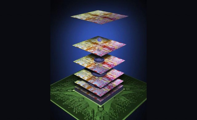
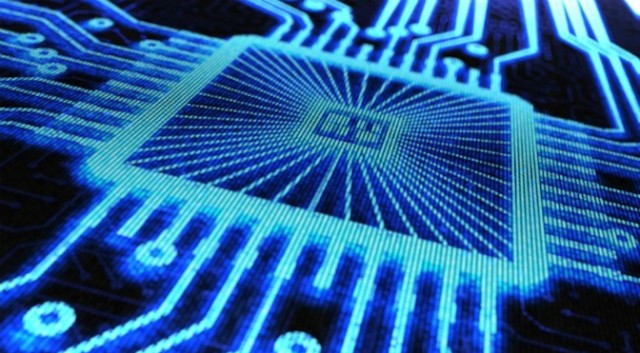
 The first commercial version of the new kind of computer chip is scheduled to be released in 2014, and was the result of a collaborative effort between I.B.M. and Qualcomm, as well as a Stanford research team. This “neuromorphic processor” can not only automate tasks that once required painstaking programming, but can also sidestep and even tolerate errors, potentially making the term “computer crash” obsolete.
In coming years, the approach will make possible a new generation of artificial intelligence systems that will perform some functions that humans do with ease: see, speak, listen, navigate, manipulate and control. That can hold enormous consequences for tasks like facial and speech recognition, navigation and planning, which are still in elementary stages and rely heavily on human programming.
 For example, computer vision systems only “recognize” objects that can be identified by the statistics-oriented algorithms programmed into them. An algorithm is like a recipe, a set of step-by-step instructions to perform a calculation. But last year, Google researchers were able to get a machine-learning algorithm, known as a “Google Neural Network”, to perform an identification task (involving cats) without supervision.
And this past June, the company said it had used those neural network techniques to develop a new search service to help customers find specific photos more accurately. And this past November, researchers at Standford University came up with a new algorithm that could give computers the power to more reliably interpret language. It’s known as the Neural Analysis of Sentiment (NaSent).
 A similar concept known as Deep Leaning is also looking to endow software with a measure of common sense. Google is using this technique with their voice recognition technology to aid in performing searches. In addition, the social media giant Facebook is looking to use deep learning to help them improve Graph Search, an engine that allows users to search activity on their network.
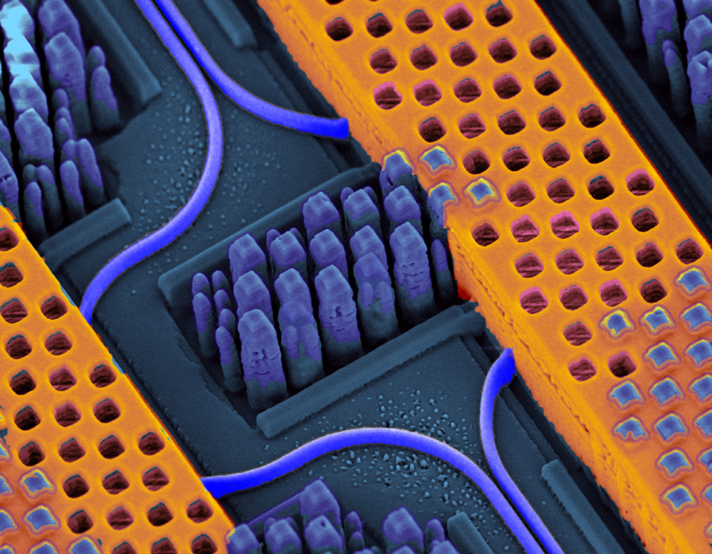
Until now, the design of computers was dictated by ideas originated by the mathematician John von Neumann about 65 years ago. Microprocessors perform operations at lightning speed, following instructions programmed using long strings of binary code (0s and 1s). The information is stored separately in what is known as memory, either in the processor itself, in adjacent storage chips or in higher capacity magnetic disk drives.
 By contrast, the new processors consist of electronic components that can be connected by wires that mimic biological synapses. Because they are based on large groups of neuron-like elements, they are known as neuromorphic processors, a term credited to the California Institute of Technology physicist Carver Mead, who pioneered the concept in the late 1980s.
These processors are not “programmed”, in the conventional sense. Instead, the connections between the circuits are “weighted” according to correlations in data that the processor has already “learned.” Those weights are then altered as data flows in to the chip, causing them to change their values and to “spike.” This, in turn, strengthens some connections and weakens others, reacting much the same way the human brain does.
 In the words of Dharmendra Modha, an I.B.M. computer scientist who leads the company’s cognitive computing research effort:
Instead of bringing data to computation as we do today, we can now bring computation to data. Sensors become the computer, and it opens up a new way to use computer chips that can be everywhere.
One great advantage of the new approach is its ability to tolerate glitches, whereas traditional computers are cannot work around the failure of even a single transistor. With the biological designs, the algorithms are ever changing, allowing the system to continuously adapt and work around failures to complete tasks. Another benefit is energy efficiency, another inspiration drawn from the human brain.
 The new computers, which are still based on silicon chips, will not replace today’s computers, but augment them; at least for the foreseeable future. Many computer designers see them as coprocessors, meaning they can work in tandem with other circuits that can be embedded in smartphones and the centralized computers that run computing clouds.
However, the new approach is still limited, thanks to the fact that scientists still do not fully understand how the human brain functions. As Kwabena Boahen, a computer scientist who leads Stanford’s Brains in Silicon research program, put it:
We have no clue. I’m an engineer, and I build things. There are these highfalutin theories, but give me one that will let me build something.
 Luckily, there are efforts underway that are designed to remedy this, with the specific intention of directing that knowledge towards the creation of better computers and AIs. One such effort comes from the National Science Foundation financed the Center for Brains, Minds and Machines, a new research center based at the Massachusetts Institute of Technology, with Harvard and Cornell.
Another is the California Institute for Telecommunications and Information Technology (aka. Calit2) – a center dedicated to innovation in nanotechnology, life sciences, information technology, and telecommunications. As
Larry Smarr, an astrophysicist and director of Institute, put it:
We’re moving from engineering computing systems to something that has many of the characteristics of biological computing.
 And last, but certainly not least, is the Human Brain Project, an international group of 200 scientists from 80 different research institutions and based in Lausanne, Switzerland. Having secured the $1.6 billion they need to fund their efforts, these researchers will spend the next ten years conducting research that cuts across multiple disciplines.
This initiative, which has been compared to the Large Hadron Collider, will attempt to reconstruct the human brain piece-by-piece and gradually bring these cognitive components into an overarching supercomputer. The expected result of this research will be new platforms for “neuromorphic computing” and “neurorobotics,” allowing for the creation of computing and robotic architectures that mimic the functions of the human brain.
 When future generations look back on this decade, no doubt they will refer to it as the birth of the neuromophic computing revolution. Or maybe just Neuromorphic Revolution for short, but that sort of depends on the outcome. With so many technological revolutions well underway, it is difficult to imagine how the future will look back and characterize this time.
Perhaps, as Charles Stross suggest, it will simply be known as “the teens”, that time in pre-Singularity history where it was all starting to come together, but was yet to explode and violently change everything we know. I for one am looking forward to being around to witness it all!
Sources: nytimes.com, technologyreview.com, calit2.net, humanbrainproject.eu

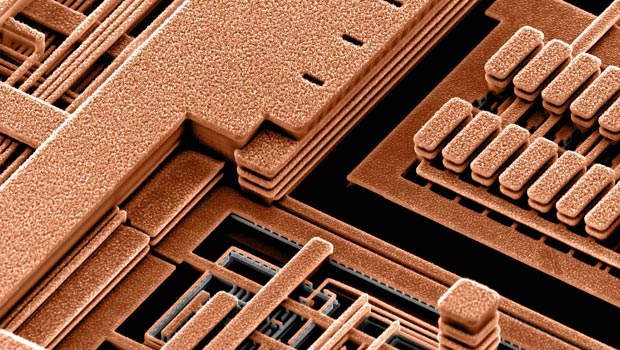
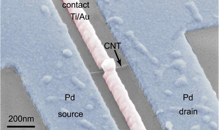
 Ask a technician or a computer science major, and they will likely tell you that the next great leap in computing will only come once Moore’s Law is overcome. This law, which states that the number of transistors on a single chip doubles every 18 months to two years, is proceeding towards a bottleneck. For decades, CPUs and computer chips have been getting smaller, but they are fast approaching their physical limitations.
 This has led scientists and engineers to propose that new materials be used, and graphene appears to be the current favorite. And researchers at the University of California at Berkeley are busy working on a form of so-called nanoribbon graphene that could increase the density of transistors on a computer chip by as much as 10,000 times.
 Work on nanoribbons over the past decade has revolved around using lasers to carefully sculpt ribbons 10 or 20 atoms wide from larger sheets of graphene. On the scale of billionths of an inch, that calls for incredible precision. If the makers are even a few carbon atoms off, it can completely alter the properties of the ribbon, preventing it from working as a semiconductor at room temperature.
 He begins by synthesizing rings of carbon atoms similar in structure to benzene, then heats the molecules to encourage them to form a long chain. A second heating step strips away most of the hydrogen atoms, freeing up the carbon to form bonds in a honeycomb-like graphene structure. This process allows Fischer and his colleagues to control where each atom of carbon goes in the final nanoribbon.