News from Space: Time Capsule to Mars

Time_capsule_to_mars1The selfie is an apparent obsession amongst today’s youth, snapping pictures of themselves and posting them to social media. But for just 99 cents, people can send a picture of themselves to the Red Planet as part of the Time Capsule to Mars (TC2M) – a student-led, crowdfunded project that aims to send three CubeSat microsatellites to the planet containing digital messages from tens of millions of people from all around around the world.

The objective of the TC2M – a project of Explore Mars – mission is to inspire people throughout the globe and allow them a personal connection with space exploration in the same spirit of the Apollo missions. The non-profit organization also aims to educate and inspire children by enabling them to upload their media content, track their spacecraft and lander, and participate in the mission via a personalized Mission Control portal over the internet.

Mars_exploreWith the help and support of NASA, MIT, Stanford University and Deep Space Industries (among others), the student-led team will design, launch, fly and land three CubeSat-based spacecraft on the surface of Mars. The projected cost of the mission, covering everything from design to launch, is $25 million, which TC2M will attempt to raise by way of crowdfunding.

In terms of sending media content, people currently have the option of uploading only images up to 10 MB in size. However, in the coming months, TC2M claims that participants will also be able to upload other types of media such as videos, audio clips and text files. In order to reach as many people as possible, uploads in the developing world will be free of charge for smaller files, underwritten by corporate sponsors.

Time_capsule_to_mars2Emily Briere, a mechanical engineering student who is heading the project, explained their aim thusly:

We hope to inspire and educate young people worldwide by enabling them to personally engage and be part of the mission. The distributed approach to funding and personal engagement will ultimately guarantee our success.

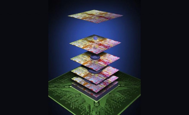
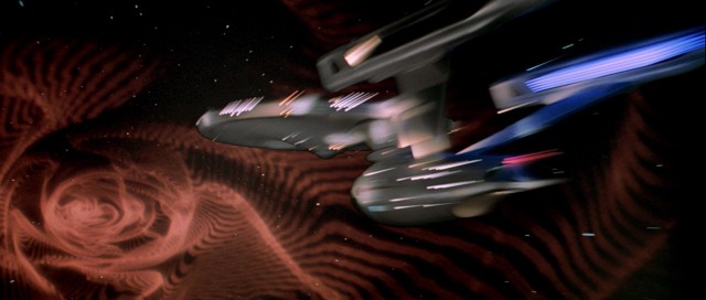
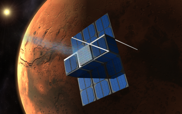
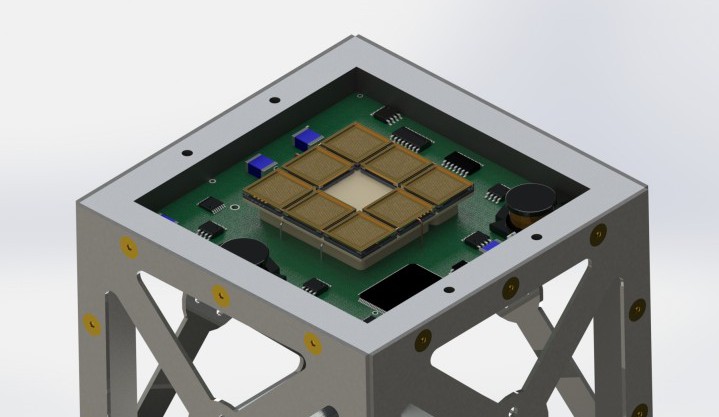
The data will be carried by three identical 13-kg (27-lb) CubeSat spacecraft, each 30 x 40 x 10 cm (12 x 16 x 4 inches) in size. This will be the first time that such spacecraft are used for interplanetary travel, as well as the first time that many of the new technologies are being tested. The data will be stored in a quartz crystal, which is extremely dense and could last for millions of years, hence making it ideal for surviving the hostile conditions on Mars.

Time_capsule_to_mars_thruster
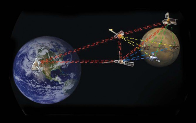
The technologies being tested on the three spacecraft include delay-tolerant networking for the Deep Space Internet, inflatable antennae, and new interplanetary radiation sensors that will pave the way for future human trips to Mars. But out of all the new technologies being tested, the most exciting is certainly the propulsion system. But the most interesting technology of all will be in the form of its engines.

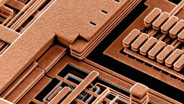
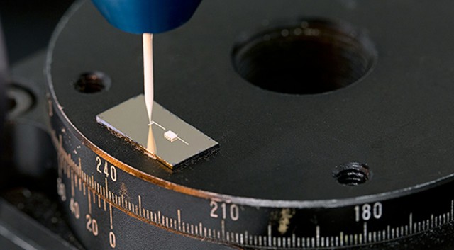
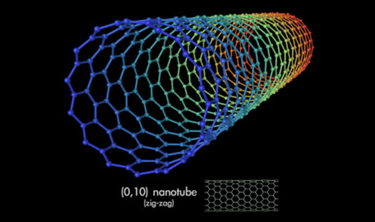
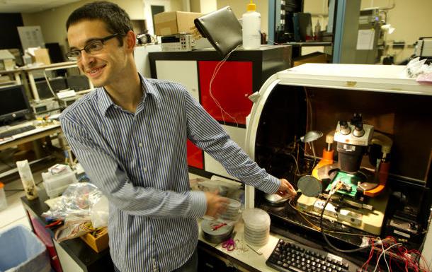
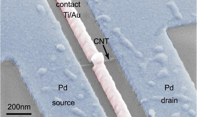
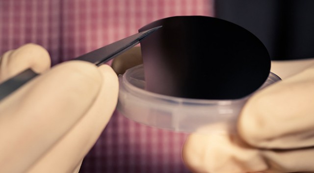
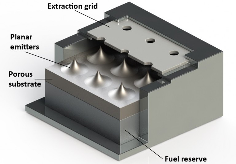
The three spacecraft will be propelled by an ion electrospray system (iEPS), a microthruster developed at MIT that is essentially size of a penny (pictured above). Each spacecraft will be powered by 40 thruster pairs, which will generate thrust using an electric field to extract and accelerate ions. The ionic liquid propellant is much more efficient than rocket fuel, and MIT scientists believe a scaled-up version may one day bring humans to Mars.

Time_capsule_to_mars_thruster1The choice of employing three separate but identical spacecraft for the mission may be due in part to the fact that so many new technologies are being tested at the same time. To triple the chances of success, Briere has previously said that crowdfunders who want to send their media to Mars will have the option of having the data uploaded on all three spacecraft, for an additional price.

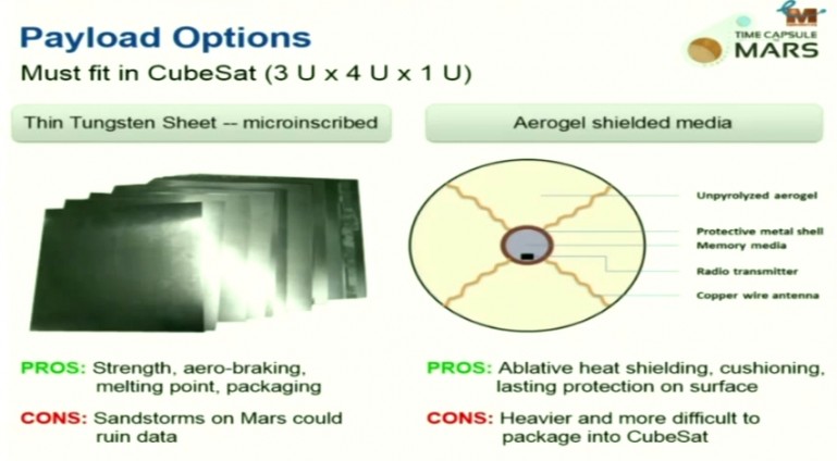
The spacecraft themselves will disintegrate as they traverse the Martian atmosphere. However, the payloads are being designed to aerobrake and land on the surface of Mars while keeping the data intact and preserved uncorrupted on the surface of the planet for a long, long time. As for how they intend to keep it stored until the day that manned missions can retrieve it, there are a few options on the table.

Time_capsule_to_marsOne option that is being considered is to use a microinscribed thin tungsten sheet, which has the advantage of being thin, light and strong, with a high melting point – meaning it won’t disintegrate upon entry – and good aerobraking properties because of its large surface area. However, there are concerns that sandstorms on Mars might damage the data once it has landed.

A second option would be an aerogel-shielded media. A metal ball could encase the data which would be stored in a very light medium, such as a quartz memory. The metal ball would be surrounded with an aerogel that will act as an ablative shield as it enters the atmosphere. And as it gets closer to the surface, the metal ball will act as a cushion for the data as it lands on Mars.

Time_capsule_to_mars3The organizers have only just announced their crowdfunding plans, and expect to reach the very ambitious goal of $25 million before the launch, which is planned for 2017. You can contribute to the mission and upload your own picture by visiting the mission website. And for those interested in possibly contributing, stay tuned to find out how and where you can donate once the crowdfunding campaign is up and running.

So in addition to showcasing new spacecraft, new media technologies, this project is also an attempt to stimulate interest in the new age of space exploration – an age characterized by public access and involvement. It’s also an opportunity to make your mark on the Red Planet, a mark which will someday (if all goes to plan) be uncovered by a new generation of explorers and settlers.

In the meantime, be sure to watch the short promotional video below which describes the mission and its goals:


Sources:
gizmag.com, timecapsuletomars.com, web.mit.edu

The Future of Computing: Brain-Like Computers

neuronsIt’s no secret that computer scientists and engineers are looking to the human brain as means of achieving the next great leap in computer evolution. Already, machines are being developed that rely on machine blood, can continue working despite being damaged, and recognize images and speech. And soon, a computer chip that is capable of learning from its mistakes will also be available.

The new computing approach, already in use by some large technology companies, is based on the biological nervous system – specifically on how neurons react to stimuli and connect with other neurons to interpret information. It allows computers to absorb new information while carrying out a task, and adjust what they do based on the changing signals.

brain_chip2The first commercial version of the new kind of computer chip is scheduled to be released in 2014, and was the result of a collaborative effort between I.B.M. and Qualcomm, as well as a Stanford research team. This “neuromorphic processor” can not only automate tasks that once required painstaking programming, but can also sidestep and even tolerate errors, potentially making the term “computer crash” obsolete.

In coming years, the approach will make possible a new generation of artificial intelligence systems that will perform some functions that humans do with ease: see, speak, listen, navigate, manipulate and control. That can hold enormous consequences for tasks like facial and speech recognition, navigation and planning, which are still in elementary stages and rely heavily on human programming.

googleneuralnetworkFor example, computer vision systems only “recognize” objects that can be identified by the statistics-oriented algorithms programmed into them. An algorithm is like a recipe, a set of step-by-step instructions to perform a calculation. But last year, Google researchers were able to get a machine-learning algorithm, known as a “Google Neural Network”, to perform an identification task (involving cats) without supervision.

And this past June, the company said it had used those neural network techniques to develop a new search service to help customers find specific photos more accurately. And this past November, researchers at Standford University came up with a new algorithm that could give computers the power to more reliably interpret language. It’s known as the Neural Analysis of Sentiment (NaSent).

deep_learning_laptopA similar concept known as Deep Leaning is also looking to endow software with a measure of common sense. Google is using this technique with their voice recognition technology to aid in performing searches. In addition, the social media giant Facebook is looking to use deep learning to help them improve Graph Search, an engine that allows users to search activity on their network.

Until now, the design of computers was dictated by ideas originated by the mathematician John von Neumann about 65 years ago. Microprocessors perform operations at lightning speed, following instructions programmed using long strings of binary code (0s and 1s). The information is stored separately in what is known as memory, either in the processor itself, in adjacent storage chips or in higher capacity magnetic disk drives.

neural-networksBy contrast, the new processors consist of electronic components that can be connected by wires that mimic biological synapses. Because they are based on large groups of neuron-like elements, they are known as neuromorphic processors, a term credited to the California Institute of Technology physicist Carver Mead, who pioneered the concept in the late 1980s.

These processors are not “programmed”, in the conventional sense. Instead, the connections between the circuits are “weighted” according to correlations in data that the processor has already “learned.” Those weights are then altered as data flows in to the chip, causing them to change their values and to “spike.” This, in turn, strengthens some connections and weakens others, reacting much the same way the human brain does.

Neuromorphic-chip-640x353In the words of Dharmendra Modha, an I.B.M. computer scientist who leads the company’s cognitive computing research effort:

Instead of bringing data to computation as we do today, we can now bring computation to data. Sensors become the computer, and it opens up a new way to use computer chips that can be everywhere.

One great advantage of the new approach is its ability to tolerate glitches, whereas traditional computers are cannot work around the failure of even a single transistor. With the biological designs, the algorithms are ever changing, allowing the system to continuously adapt and work around failures to complete tasks. Another benefit is energy efficiency, another inspiration drawn from the human brain.

IBM_stacked3dchipsThe new computers, which are still based on silicon chips, will not replace today’s computers, but augment them; at least for the foreseeable future. Many computer designers see them as coprocessors, meaning they can work in tandem with other circuits that can be embedded in smartphones and the centralized computers that run computing clouds.

However, the new approach is still limited, thanks to the fact that scientists still do not fully understand how the human brain functions. As Kwabena Boahen, a computer scientist who leads Stanford’s Brains in Silicon research program, put it:

We have no clue. I’m an engineer, and I build things. There are these highfalutin theories, but give me one that will let me build something.

calit2PhotoLuckily, there are efforts underway that are designed to remedy this, with the specific intention of directing that knowledge towards the creation of better computers and AIs. One such effort comes from the National Science Foundation financed the Center for Brains, Minds and Machines, a new research center based at the Massachusetts Institute of Technology, with Harvard and Cornell.

Another is the California Institute for Telecommunications and Information Technology (aka. Calit2) – a center dedicated to innovation in nanotechnology, life sciences, information technology, and telecommunications. As
Larry Smarr, an astrophysicist and director of Institute, put it:

We’re moving from engineering computing systems to something that has many of the characteristics of biological computing.

Human-Brain-project-Alp-ICTAnd last, but certainly not least, is the Human Brain Project, an international group of 200 scientists from 80 different research institutions and based in Lausanne, Switzerland. Having secured the $1.6 billion they need to fund their efforts, these researchers will spend the next ten years conducting research that cuts across multiple disciplines.

This initiative, which has been compared to the Large Hadron Collider, will attempt to reconstruct the human brain piece-by-piece and gradually bring these cognitive components into an overarching supercomputer. The expected result of this research will be new platforms for “neuromorphic computing” and “neurorobotics,” allowing for the creation of computing and robotic architectures that mimic the functions of the human brain.

neuromorphic_revolutionWhen future generations look back on this decade, no doubt they will refer to it as the birth of the neuromophic computing revolution. Or maybe just Neuromorphic Revolution for short, but that sort of depends on the outcome. With so many technological revolutions well underway, it is difficult to imagine how the future will look back and characterize this time.

Perhaps, as Charles Stross suggest, it will simply be known as “the teens”, that time in pre-Singularity history where it was all starting to come together, but was yet to explode and violently change everything we know. I for one am looking forward to being around to witness it all!

Sources: nytimes.com, technologyreview.com, calit2.net, humanbrainproject.eu

Year-End Tech News: Stanene and Nanoparticle Ink

3d.printingThe year of 2013 was also a boon for the high-tech industry, especially where electronics and additive manufacturing were concerned. In fact, several key developments took place last year that may help scientists and researchers to move beyond Moore’s Law, as well as ring in a new era of manufacturing and production.

In terms of computing, developers have long feared that Moore’s Law – which states that the number of transistors on integrated circuits doubles approximately every two years – could be reaching a bottleneck. While the law (really it’s more of an observation) has certainly held true for the past forty years, it has been understood for some time that the use of silicon and copper wiring would eventually impose limits.

copper_in_chips__620x350Basically, one can only miniaturize circuits made from these materials so much before resistance occurs and they are too fragile to be effective. Because of this, researchers have been looking for replacement materials to substitute the silicon that makes up the 1 billion transistors, and the one hundred or so kilometers of copper wire, that currently make up an integrated circuit.

Various materials have been proposed, such as graphene, carbyne, and even carbon nanotubes. But now, a group of researchers from Stanford University and the SLAC National Accelerator Laboratory in California are proposing another material. It’s known as Stanene, a theorized material fabricated from a single layer of tin atoms that is theoretically extremely efficient, even at high temperatures.

computer_chip5Compared to graphene, which is stupendously conductive, the researchers at Stanford and the SLAC claim that stanene should be a topological insulator. Topological insulators, due to their arrangement of electrons/nuclei, are insulators on their interior, but conductive along their edge and/or surface. Being only a single atom in thickness along its edges, this topological insulator can conduct electricity with 100% efficiency.

The Stanford and SLAC researchers also say that stanene would not only have 100%-efficiency edges at room temperature, but with a bit of fluorine, would also have 100% efficiency at temperatures of up to 100 degrees Celsius (212 Fahrenheit). This is very important if stanene is ever to be used in computer chips, which have operational temps of between 40 and 90 C (104 and 194 F).

Though the claim of perfect efficiency seems outlandish to some, others admit that near-perfect efficiency is possible. And while no stanene has been fabricated yet, it is unlikely that it would be hard to fashion some on a small scale, as the technology currently exists. However, it will likely be a very, very long time until stanene is used in the production of computer chips.

Battery-Printer-640x353In the realm of additive manufacturing (aka. 3-D printing) several major developments were made during the year 0f 2013. This one came from Harvard University, where a materials scientist named Jennifer Lewis Lewis – using currently technology – has developed new “inks” that can be used to print batteries and other electronic components.

3-D printing is already at work in the field of consumer electronics with casings and some smaller components being made on industrial 3D printers. However, the need for traditionally produced circuit boards and batteries limits the usefulness of 3D printing. If the work being done by Lewis proves fruitful, it could make fabrication of a finished product considerably faster and easier.

3d_batteryThe Harvard team is calling the material “ink,” but in fact, it’s a suspension of nanoparticles in a dense liquid medium. In the case of the battery printing ink, the team starts with a vial of deionized water and ethylene glycol and adds nanoparticles of lithium titanium oxide. The mixture is homogenized, then centrifuged to separate out any larger particles, and the battery ink is formed.

This process is possible because of the unique properties of the nanoparticle suspension. It is mostly solid as it sits in the printer ready to be applied, then begins to flow like liquid when pressure is increased. Once it leaves the custom printer nozzle, it returns to a solid state. From this, Lewis’ team was able to lay down multiple layers of this ink with extreme precision at 100-nanometer accuracy.

laser-welding-640x353The tiny batteries being printed are about 1mm square, and could pack even higher energy density than conventional cells thanks to the intricate constructions. This approach is much more realistic than other metal printing technologies because it happens at room temperature, no need for microwaves, lasers or high-temperatures at all.

More importantly, it works with existing industrial 3D printers that were built to work with plastics. Because of this, battery production can be done cheaply using printers that cost on the order of a few hundred dollars, and not industrial-sized ones that can cost upwards of $1 million.

Smaller computers, and smaller, more efficient batteries. It seems that miniaturization, which some feared would be plateauing this decade, is safe for the foreseeable future! So I guess we can keep counting on our electronics getting smaller, harder to use, and easier to lose for the next few years. Yay for us!

Sources: extremetech.com, (2)

The Future of Physics: Entanglements and Wormholes

worm_holeQuantum entanglements are one of the most bizarre aspects of quantum physics, so much so that Albert Einstein himself referred to it as “spooky action at a distance.” Basically, the concept involves two particles with each occupying multiple states at once. Until such time as one is measured, neither has a definite state, causing the other particle to instantly assume a corresponding state, even if they reside on opposite ends of the universe.

But what enables particles to communicate instantaneously – and seemingly faster than the speed of light – over such vast distances? Earlier this year, physicists proposed an answer in the form of “wormholes,” or gravitational tunnels. The group showed that by creating two entangled black holes, then pulling them apart, they formed a wormhole connecting the distant black holes.

quantum-entanglement1Now an MIT physicist has found that, looked at through the lens of string theory, the creation of two entangled quarks — the very building blocks of matter — simultaneously gives rise to a wormhole connecting the pair. The theoretical results bolster the relatively new and exciting idea that the laws of gravity that hold the universe together may not be fundamental, but may arise from quantum entanglement themselves.

Julian Sonner, a senior postdoc at MIT’s Laboratory for Nuclear Science and Center for Theoretical Physics, published the results of his study in the journal Physical Review Letters, where it appears together with a related paper by Kristan Jensen of the University of Victoria and Andreas Karch of the University of Washington. Already, the theory is causing quite the buzz for scientists and fans of sci-fi who would like to believe FTL is still possible.

quantum_field_theoryThis is certainly good news for scientists looking to resolve the fundamental nature of the universe by seeing how its discernible laws fit together. Ever since quantum mechanics was first proposed more than a century ago, the main challenge for physicists has been to explain how it correlates to gravity. While quantum mechanics works extremely well at describing how things work on the microscopic level, it remains incompatible with general relativity.

For years, physicists have tried to come up with a theory that can marry the two fields. This has ranged from proposing the existence of a subatomic particle known as the “graviton” or “dilaton”, to various Grand Unifying Theories – aka. Theory of Everything (TOE) – such as Superstring Theory, Loop Quantum Gravity, and other theoretical models to explain the interaction. But so far, none have proven successful.

gravity_well_cartography_2_by_lordsong-d5lrxwsA theory of quantum gravity would suggest that classical gravity is not a fundamental concept, as Einstein first proposed, but rather emerges from a more basic, quantum-based phenomenon. In a macroscopic context, this would mean that the universe is shaped by something more fundamental than the forces of gravity. This is where quantum entanglement could play a role.

Naturally, there is a problem with this idea. Two entangled particles, “communicating” across vast distances, would have to do so at speeds faster than that of light — a violation of the laws of physics, according to Einstein. In July, physicists Juan Maldacena of the Institute for Advanced Study and Leonard Susskind of Stanford University proposed a theoretical solution in the form of two entangled black holes.

big bang_blackholeWhen the black holes were entangled, then pulled apart, the theorists found that what emerged was a wormhole – a tunnel through space-time that is thought to be held together by gravity. The idea seemed to suggest that, in the case of wormholes, gravity emerges from the more fundamental phenomenon of entangled black holes. Following up on work by Jensen and Karch, Sonner has sought to tackle this idea at the level of quarks.

To see what emerges from two entangled quarks, he first generated entangled quarks using the Schwinger effect — a concept in quantum theory that enables one to create particles out of nothing. Sonner then mapped the entangled quarks onto a four-dimensional space, considered a representation of space-time. In contrast, gravity is thought to exist in the fifth dimension. According to Einstein’s laws, it acts to “bend” and shape space-time.

black_holeTo see what geometry may emerge in the fifth dimension from entangled quarks in the fourth, Sonner employed holographic duality, a concept in string theory. While a hologram is a two-dimensional object, it contains all the information necessary to represent a three-dimensional view. Essentially, holographic duality is a way to derive a more complex dimension from the next lowest dimension.

Using holographic duality, Sonner derived the entangled quarks, and found that what emerged was a wormhole connecting the two, implying that the creation of quarks simultaneously creates a wormhole between them. More fundamentally, the results suggest that gravity itself may emerge from quantum entanglement. On top of all that, the geometry, or bending, of the universe as described by classical gravity, may also be a consequence of entanglement.

quantum-entanglement3As Sonner put it in his report, the results are a theoretical explanation for a problem that has dogged scientists who quite some time:

There are some hard questions of quantum gravity we still don’t understand, and we’ve been banging our heads against these problems for a long time. We need to find the right inroads to understanding these questions… It’s the most basic representation yet that we have where entanglement gives rise to some sort of geometry. What happens if some of this entanglement is lost, and what happens to the geometry? There are many roads that can be pursued, and in that sense, this work can turn out to be very helpful.

Granted, the idea of riding wormholes so that we, as humans, can travel from one location in space to another is still very much science fiction, knowing that there may very well be a sound, scientific basis for their existence is good news for anyone who believes we will be able to “jump” around the universe in the near to distant future. I used to be one of them, now… I think I might just be a believer again!

USS_Enterprise_caught_in_artificial_wormhole-640x272Sources: web.mit.edu, extremetech.com

The Future is Here: Carbon Nanotube Computers

carbon-nanotubeSilicon Valley is undergoing a major shift, one which may require it to rethink its name. This is thanks in no small part to the efforts of a team based at Stanford that is seeking to create the first basic computer built around carbon nanotubes rather than silicon chips. In addition to changing how computers are built, this is likely to extend the efficiency and performance.

What’s more, this change may deal a serious blow to the law of computing known as Moore’s Law. For decades now, the exponential acceleration of technology – which has taken us from room-size computers run by punched paper cards to handheld devices with far more computing power – has depended the ability to place more and more transistors onto an individual chip.

PPTMooresLawaiThe result of this ongoing trend in miniaturization has been devices that are becoming smaller, more powerful, and cheaper. The law used to describe this – though “basic rule” would be a more apt description – states that the number of transistors on a chip has been doubling every 18 months or so since the dawn of the information age. This is what is known as “Moore’s Law.”

However, this trend could be coming to an end, mainly because its becoming increasingly difficult, expensive and inefficient to keep jamming more tiny transistors on a chip. In addition, there are the inevitable physical limitations involved, as miniaturization can only go on for so long before its becomes unfeasible.

carbon_nanotubecomputerCarbon nanotubes, which are long chains of carbon atoms thousands of times thinner than a human hair, have the potential to be more energy-efficient and outperform computers made with silicon components. Using a technique that involved “burning” off and weeding out imperfections with an algorithm from the nanotube matrix, the team built a very basic computer with 178 transistors that can do tasks like counting and number sorting.

In a recent release from the university, Stanford professor Subhasish Mitra said:

People have been talking about a new era of carbon nanotube electronics moving beyond silicon. But there have been few demonstrations of complete digital systems using this exciting technology. Here is the proof.

Naturally, this computer is more of a proof of concept than a working prototype. There are still a number of problems with the idea, such as the fact that nanotubes don’t always grow in straight lines and cannot always “switch off” like a regular transistor. The Stanford team’s computer’s also has limited power due to the limited facilities they had to work with, which did not have access to industrial fabrication tools.

carbon_nanotube2All told, their computer is only about as powerful as an Intel 4004, the first single-chip silicon microprocessor that was released in 1971. But given time, we can expect more sophisticated designs to emerge, especially if design teams have access to top of the line facilities to build prototypes.

And this research team is hardly alone in this regard. Last year, Silicon Valley giant IBM managed to create their own transistors using carbon nanotubes and also found that they outperformed the transistors made of silicon. What’s more, these transistors measured less than ten nanometers across, and were able to operated using very low voltage.

carbon_nanotube_transistorSimilarly, a research team from Northwestern University in Evanston, Illinois managed to create something very similar. In their case, this consisted of a logic gate – the fundamental circuit that all integrated circuits are based on – using carbon nanotubes to create transistors that operate in a CMOS-like architecture. And much like IBM and the Standford team’s transistors, it functioned at very low power levels.

What this demonstrated is that carbon nanotube transistors and other computer components are not only feasible, but are able to outperform transistors many times their size while using a fraction of the power. Hence, it is probably only a matter of time before a fully-functional computer is built – using carbon nanotube components – that will supersede silicon systems and throw Moore’s Law out the window.

Sources: news.cnet.com, (2), fastcolabs.com

Judgement Day Update: Headless Ape Bot

robosimianIt goes by the name of Robosimian, an ape-like robot that was built by NASA’s Jet Propulsion Laboratory. Designed and built by JPL and Stanford engineers, RoboSimian was a recent competitor in the DARPA Robotics Challenge, a competition where participants attempt to create strong, dextrous, and flexible robots that could aid in disasters as well as search and rescue missions.

Admittedly, the robot looks kind of creepy, due in no small part to the fact that it doesn’t have a head. But keep in mind, this machine is designed to save your life. As part of the DARPA challenge, they are intended to go places that would be too dangerous for humans. So I imagine whatever issues a person may have with its aesthetics would disappear when they spotted one crawling to their rescue.

robosimian1To win the challenge, the semi-autonomous robots will have to complete difficult tasks that demonstrate its dexterity and ambulatory ability. These include removing debris from a doorway, using a tool to break through a concrete panel, connecting a fire hose to a pipe and turning it on, and driving a vehicle at a disaster site. The competition, which began in 2012, will have its first trials in December.

Many of the teams in the challenge are creating fairly humanoid robots but RoboSimian, as its name implies, looks a bit more like an ape. And there is a reason for this: relying on four very flexible limbs, each of which has a three-fingered hand, the robot is much better suited to climbing and hanging, much like our Simian cousins. This makes it well-suited for the DARPA-set requirement of climbing a ladder, and will no doubt come in handy when the robot has to navigate difficult environments.

Robosimian2The demo video, featured below, shows the robots hands doing dextrous tasks as well as doing some pull ups. There’s also a computer renderings of what the final machine may look like. Check it out:


Source: wired.com

Powered by the Sun: Nanotech Solar Cells

???????????????????????????????????????????????????????????????????????????????????????????????????????????????????????????????????????????????????????????????????????????????????????????????????????????????????????????????????????????????????????????????????????????????????????????????????????????????????????????????????????????????????????????????????????????????????????????????????????????????????????????????????????????With every passing year, interest in solar power has been growing by leaps and bounds. Given the impacts of Climate Change, widespread droughts, tropical storms, wildfires and increasing global temperatures, this should not come as a surprise. But an equally important factor in the adoption of clean energy alternatives has to do with improvements that are being made which will make it more efficient, accessible, and appealing to power companies and consumers.

Three such recent developments come to us from Standford, MIT, and the Neils Bohr Institute, respectively; where researchers have announced new ways using nanoprocesses to boost the yield of individual solar cells. In addition to cutting costs associated with production, installation, and storage, increasing the overall electrical yield of solar cells is a major step towards their full-scale implementation.

solar_nanoFirst, there’s MIT’s new concept for a solar cell, which uses nanowires to massively boost the efficiency of quantum dot photovoltaic cells. Quantum dots – which are basically nano-sized crystals of a semiconducting material – are already being considered as an alternative to conventional silicon cells, since they are cheaper and easier to produce.

However, until recently they have been a letdown in the efficiency department, lagging significantly behind their silicon counterparts. By merging zinc oxide nanowires into the design of their quantum dot photovoltaic cells, the MIT researchers were able to boost the current produced by 50%, and overall efficiency by 5%.  Ultimately, their goal is to get that up to 10%, since that is considered to be the threshold for commercial adoption.

gallium-arsenide-nanowire-solar-cellMeanwhile, researchers at the Niels Bohr Institute in Denmark and EPFL in Switzerland announced that they have built solar cells out of single nanowires. In this case, the process involved growing gallium-arsenide (GaAs) wires on a silicon substrate, and then completing the circuit with a transparent indium tin oxide electrode, which are currently employed in the creation of photovoltaic cells and LEDs on the market today.

Prior to these development, nanowires were being researched mainly in conjunction with computer chips as a possible replacement for silicon. But thanks to the combined work of these researchers, we may very well be looking at solar cells which are not only hair-thin (as with the kind being developed by Penn State University) but microscopically thin. And much like the research at the University of Oslo involving the use of microbeads, this too will mean the creation of ultra-thin solar cells that have a massive energy density – 180 mA/cm2, versus ~40 mA/cm2 for crystalline silicon PVs.

solar_boosterAnd last, but not least, there was the announcement from Stanford University of a revolutionary new type of solar cell that has doubled the efficiency of traditional photovoltaic cells. This new device uses a process called photon-enhanced thermionic emission (PETE) that allows for the absorption of not only light, but heat. This combination makes this new type of cell the equivalent of a turbocharged solar panel!

pete-photovoltaic-thermionic-diagram-stanfordIn conventional cells, photons strike a semiconductor (usually silicon), creating electricity by knocking electrons loose from their parent atoms. The PETE process, on the other hand, uses the gallium arsenide wafer on top gather as much sunlight as possible, creating a lot of excited electrons using the photovoltaic effect. The underside, which is composed of nanoantennae, emits these photoexcited electrons across a vacuum to the anode with gathers them and turns them into an electrical current.

Beneath the anode is a of heat pipe that collects any leftover heat which could be used elsewhere. One of the easiest applications of PETE would be in concentrating solar power plants, where thousands of mirrors concentrate light on a central vat of boiling water, which drives a steam turbine. By concentrating the light on PETE devices instead, Stanford estimates that their power output could increase by 50%, bringing the cost of solar power generation down into the range of fossil fuels.

Though there are still kinks in their design – the cell has a very low 2% rate of energy efficient thus far – the researchers at Stanford are making improvements which are increasing its efficiency exponentially. And although their planned upgrades should lead to a solar cell capable of operating in extremely hot environments, they stress that the goal here is to build one that is capable of gathering power in non-desert environments, such as Spaced-Based solar arrays.

Combined with improved production methods, storage capacities, and plans to mount solar arrays in a variety of new places (such as on artificial islands), we could be looking at the wholesale adoption of solar power within a few years time. Every day, it seems, new methods are being unveiled that will allow Solar to supplant fossil fuels as the best, cheapest and most efficient means of energy production. If all goes as planned, all this could be coming just in time to save the planet, fingers crossed!

Sources: Extremetech.com, (2)

The Future is Here: Peel and Stick Solar Panels!

solar_arrayEver since Albert Einstein first proposed the concept in 1921, photovoltaic cells – solar cells – have been at the forefront of alternative fuel and energy research. And while progress has been made, two key factors have remained as stumbling blocks to their widespread adoption: One, the cost of making solar cells; and two, the cost of installing them.

In order for this to change, analysts have predicted for some time that solar panels would need to be printed on cheap, durable materials that could be installed anywhere. Until such time, they would continue to lose out against the gas and coal equivalents, which would continue to generate as much energy as a single solar cell while remaining comparatively cheaper.

solar_powerAnd as it turns out, the wait may be coming to an end. According to Silvija Gradecak, a materials science and engineering professor at MIT, new research from around the world is driving us ever closer to that goal. And it is her lab, among others, that is making a major contribution, through the release of a new breed of bendy, peel-and-stick solar panels.

The focus of Gradecak’s team has been on the production of a organic, thin-film cells that are made from abundant materials which could be manufactured on the cheap. And in December of last year, they made a breakthrough with the production of a transparent photovoltaic cell by using flexible graphene and a nanowire coating. This thin, flexible and transparent photo cell, they claimed, could be mounted anywhere and is comparatively cheaper than current silicon based varieties.

solar_cellNaturally, Gradecak was sure to point out that this development did not take place in a vacuum. Nor was it the only one of its kind:

“”There was a significant effort to develop these type of devices and the slope of this improvement is very high… I personally believe this is not just theoretical. In a couple of years you will see these types of devices commercially.”

And in that respect, she is right. At Stanford, researchers presented their own concept for a next generation solar cell this past December: a flexible, peel-off panel that can stick to almost any surface. Composed of nickel, silicon and silicon dioxide and a protective polymer layer, the cell consists of multiple layers that can be peeled away and applied as needed.

Exciting times, these are, especially when long-awaited environmental solutions are finally becoming feasible. It also inspires hope that we might be able to tackle a little problem known as emissions before it is too late. Of course, that would require making this technology available worldwide, especially in developing economies where coal and gas power are especially lucrative. But anything is doable, especially if the price is right!

Source: Co.Exist.com