Nanotech News: Smart Sponges, Nanoparticles and Neural Dust!

nanomachineryNanotechnology has long been the dream of researchers, scientists and futurists alike, and for obvious reasons. If machinery were small enough so as to be microscopic, or so small that it could only be measured on the atomic level,  just about anything would be possible. These include constructing buildings and products from the atomic level up, with would revolutionize manufacturing as we know it.

In addition, microscopic computers, smart cells and materials, and electronics so infinitesimally small that they could be merged with living tissues would all be within our grasp. And it seems that at least once a month, universities, research labs, and even independent skunkworks are unveiling new and exciting steps that are bringing us ever closer to this goal.

Close-up of a smart sponge

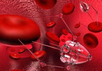
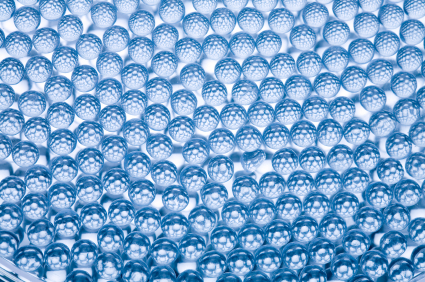
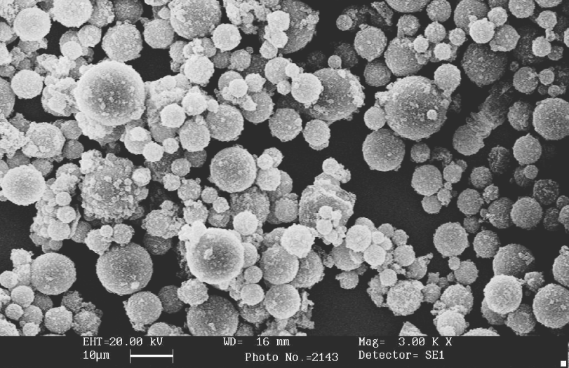
Once such breakthrough comes from the University of North Carolina at Chapel Hill, where biomedical scientists and engineers have joined forces to create the “smart sponge”. A spherical object that is microscopic — just 250 micrometers across, and could be made as small as 0.1 micrometers – these new sponges are similar to nanoparticles, in that they are intended to be the next-generation of delivery vehicles for medication.

Each sponge is mainly composed of a polymer called chitosan, something which is not naturally occurring, but can be produced easily from the chitin in crustacean shells. The long polysaccharide chains of chitosan form a matrix in which tiny porous nanocapsules are embedded, and which can be designed to respond to the presence of some external compound – be it an enzyme, blood sugar, or a chemical trigger.

bloodstreamSo far, the researchers tested the smart sponges with insulin, so the nanocapsules in this case contained glucose oxidase. As the level of glucose in a diabetic patient’s blood increases, it would trigger the nanocapsules in the smart sponge begin releasing hydrogen ions which impart a positive charge to the chitosan strands. This in turn causes them to spread apart and begin to slowly release insulin into the blood.

The process is also self-limiting: as glucose levels in the blood come down after the release of insulin, the nanocapsules deactivate and the positive charge dissipates. Without all those hydrogen ions in the way, the chitosan can come back together to keep the remaining insulin inside. The chitosan is eventually degraded and absorbed by the body, so there are no long-term health effects.

NanoparticlesOne the chief benefits of this kind of system, much like with nanoparticles, is that it delivers medication when its needed, to where its needed, and in amounts that are appropriate to the patient’s needs. So far, the team has had success treating diabetes in rats, but plans to expand their treatment to treating humans, and branching out to treat other types of disease.

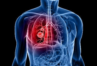
Cancer is a prime candidate, and the University team believes it can be treated without an activation system of any kind. Tumors are naturally highly acidic environments, which means a lot of free hydrogen ions. And since that’s what the diabetic smart sponge produces as a trigger anyway, it can be filled with small amounts of chemotherapy drugs that would automatically be released in areas with cancer cells.

nanorobot
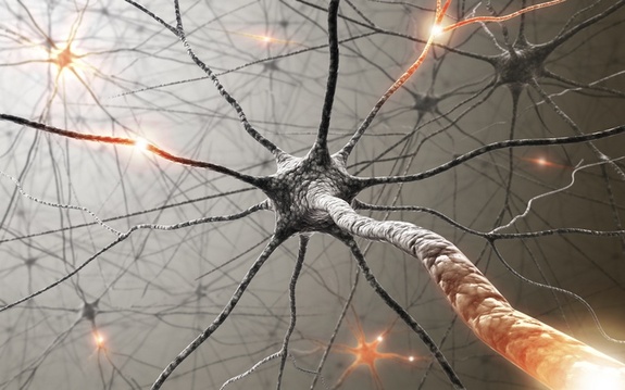
Another exciting breakthrough comes from University of California at Berkeley, where medical researchers are working towards tiny, implantable sensors . As all medical researchers know, the key to understanding and treating neurological problems is to gather real-time and in-depth information on the subject’s brain. Unfortunately, things like MRIs and positron emission tomography (PET) aren’t exactly portable and are expensive to run.

Implantable devices are fast becoming a solution to this problem, offering real-time data that comes directly from the source and can be accessed wirelessly at any time. So far, this has taken the form of temporary medical tattoos or tiny sensors which are intended to be implanted in the bloodstreams. However, what the researchers at UofC are proposing something much more radical.

neural_dust
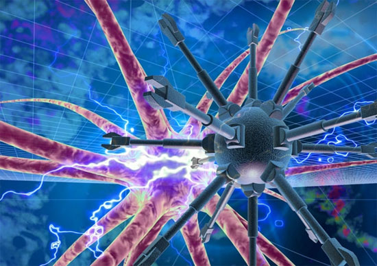
In a recent research paper, they proposed a design for a new kind of implantable sensor – an intelligent dust that can infiltrate the brain, record data, and communicate with the outside world. The preliminary design was undertaken by Berkeley’s Dongjin Seo and colleagues, who described a network of tiny sensors – each package being no more than 100 micrometers – in diameter. Hence the term they used: “neural dust”.

The smart particles would all contain a very small CMOS sensor capable of measuring electrical activity in nearby neurons. The researchers also envision a system where each particle is powered by a piezoelectric material rather than tiny batteries. The particles would communicate data to an external device via ultrasound waves, and the entire package would also be coated in a polymer, thus making it bio-neutral.

smart_tatoosBut of course, the dust would need to be complimented by some other implantable devices. These would likely include a larger subdural transceiver that would send the ultrasound waves to the dust and pick up the return signal. The internal transceiver would also be wirelessly connected to an external device on the scalp that contains data processing hardware, a long range transmitter, storage, and a battery.

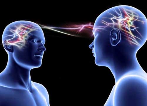
The benefits of this kind of system are again obvious. In addition to acting like an MRI running in your brain all the time, it would allow for real-time monitoring of neurological activity for the purposes of research and medical monitoring. The researchers also see this technology as a way to enable brain-machine interfaces, something which would go far beyond current methods. Who knows? It might even enable a form of machine-based telepathy in time.

telepathySounds like science fiction, and it still is. Many issues need to be worked out before something of this nature would be possible or commercially available. For one, more powerful antennae would need to be designed on the microscopic scale in order for the smart dust particles to be able to send and receive ultrasound waves.

Increasing the efficiency of transceivers and piezoelectric materials will also be a necessity to provide the dust with power, otherwise they could cause a build-up of excess heat in the user’s neurons, with dire effects! But most importantly of all, researchers need to find a safe and effective way to deliver the tiny sensors to the brain.

prosthetic_original
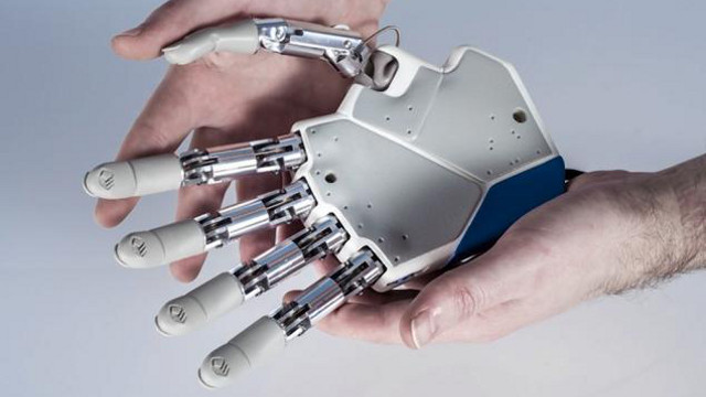
And last, but certainly not least, nanotechnology might be offering improvements in the field of prosthetics as well. In recent years, scientists have made enormous breakthroughs in the field of robotic and bionic limbs, restoring ambulatory mobility to accident victims, the disabled, and combat veterans. But even more impressive are the current efforts to restore sensation as well.

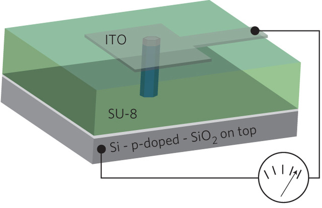
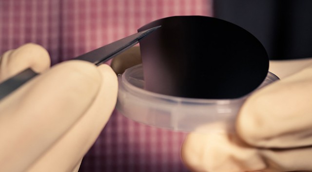
One method, which is being explored by the Technion-Israel Institute of Technology in Israel, involves incorporating gold nanoparticles and a substrate made of polyethylene terephthalate (PET) – the plastic used in bottles of soft drinks. Between these two materials, they were able to make an ultra-sensitive film that would be capable of transmitting electrical signals to the user, simulating the sensation of touch.

gold_nanoparticlesBasically, the gold-polyester nanomaterial experiences changes in conductivity as it is bent, providing an extremely sensitive measure of physical force. Tests conducted on the material showed that it was able to sense pressures ranging from tens of milligrams to tens of grams, which is ten times more sensitive than any sensors being build today.

Even better, the film maintained its sensory resolution after many “bending cycles”, meaning it showed consistent results and would give users a long term of use. Unlike many useful materials that can only really be used under laboratory conditions, this film can operate at very low voltages, meaning that it could be manufactured cheaply and actually be useful in real-world situations.

smart-skin_610x407In their research paper, lead researcher Hossam Haick described the sensors as “flowers, where the center of the flower is the gold or metal nanoparticle and the petals are the monolayer of organic ligands that generally protect it.” The paper also states that in addition to providing pressure information (touch), the sensors in their prototype were also able to sense temperature and humidity.

But of course, a great deal of calibration of the technology is still needed, so that each user’s brain is able to interpret the electronic signals being received from the artificial skin correctly. But this is standard procedure with next-generation prosthetic devices, ones which rely on two-way electronic signals to provide control signals and feedback.

nanorobot1And these are just some examples of how nanotechnology is seeking to improve and enhance our world. When it comes to sensory and mobility, it offers solutions to not only remedy health problems or limitations, but also to enhance natural abilities. But the long-term possibilities go beyond this by many orders of magnitude.

As a cornerstone to the post-singularity world being envisioned by futurists, nanotech offers solutions to everything from health and manufacturing to space exploration and clinical immortality. And as part of an ongoing trend in miniaturization, it presents the possibility of building devices and products that are even tinier and more sophisticated than we can currently imagine.

It’s always interesting how science works by scale, isn’t it? In addition to dreaming large – looking to build structures that are bigger, taller, and more elaborate – we are also looking inward, hoping to grab matter at its most basic level. In this way, we will not only be able to plant our feet anywhere in the universe, but manipulate it on the tiniest of levels.

As always, the future is a paradox, filling people with both awe and fear at the same time.

Sources: extremetech.com, (2), (3)

The Future is Here: Smart Skin!

neuronsWhen it comes to modern research and development, biomimetics appear to be the order of the day. By imitating the function of biological organisms, researchers seek to improve the function of machinery to the point that it can be integrated into human bodies. Already, researchers have unveiled devices that can do the job of organs, or bionic limbs that use the wearer’s nerve signals or thoughts to initiate motion.

But what of machinery that can actually send signals back to the user, registering pressure and stimulation? That’s what researchers from the University of Georgia have been working on of late, and it has inspired them to create a device that can do the job of the largest human organ of them all – our skin. Back in April, they announced that they had successfully created a brand of “smart skin” that is sensitive enough to rival the real thing.

smart-skin_610x407In essence, the skin is a transparent, flexible arrays that uses 8000 touch-sensitive transistors (aka. taxels) that emit electricity when agitated. Each of these comprises a bundle of some 1,500 zinc oxide nanowires, which connect to electrodes via a thin layer of gold, enabling the arrays to pick up on changes in pressure as low as 10 kilopascals, which is what human skin can detect.

Mimicking the sense of touch electronically has long been the dream researchers, and has been accomplished by measuring changes in resistance. But the team at Georgia Tech experimented with a different approach, measuring tiny polarization changes when piezoelectric materials such as zinc oxide are placed under mechanical stress. In these transistors, then, piezoelectric charges control the flow of current through the nanowires.

nanowiresIn a recent news release, lead author Zhong Lin Wang of Georgia Tech’s School of Materials Science and Engineering said:

Any mechanical motion, such as the movement of arms or the fingers of a robot, could be translated to control signals. This could make artificial skin smarter and more like the human skin. It would allow the skin to feel activity on the surface.

This, when integrated to prosthetics or even robots, will allow the user to experience the sensation of touch when using their bionic limbs. But the range of possibilities extends beyond that. As Wang explained:

This is a fundamentally new technology that allows us to control electronic devices directly using mechanical agitation. This could be used in a broad range of areas, including robotics, MEMS, human-computer interfaces, and other areas that involve mechanical deformation.

prostheticNot the first time that bionic limbs have come equipped with electrodes to enable sensation. In fact, the robotic hand designed by Silvestro Micera of the Ecole Polytechnique Federale de Lausanne in Switzerland seeks to do the same thing. Using electrodes that connect from the fingertips, palm and index finger to the wearer’s arm nerves, the device registers pressure and tension in order to help them better interact with their environment.

Building on these two efforts, it is easy to get a glimpse of what future prosthetic devices will look like. In all likelihood, they will be skin-colored and covered with a soft “dermal” layer that is studded with thousands of sensors. This way, the wearer will be able to register sensations – everything from pressure to changes in temperature and perhaps even injury – from every corner of their hand.

As usual, the technology may have military uses, since the Defense Advanced Research Projects Agency (DARPA) is involved. For that matter, so is the U.S. Air Force, the U.S. Department of Energy, the National Science Foundation, and the Knowledge Innovation Program of the Chinese Academy of Sciences are all funding it. So don’t be too surprised if bots wearing a convincing suit of artificial skin start popping up in your neighborhood!

terminator2Source: news.cnet.com

Building the Future: 3D Printing and Silkworms

arcology_crystalWhen it comes to building the homes, apartment blocks and businesses headquarters of the future,  designers and urban planners are forced to contend with a few undeniable realities. No only are these buildings going to be need to be greener and more sustainable, they will need to be built in such a way that doesn’t unnecessarily burden the environment.

Currently, the methods for erecting a large city building are criminally inefficient. Between producing the building materials – concrete, steel, wood, granite – and putting it all together, a considerable amount of energy is expended in the form of emissions and electricity, and several tons of waste are produced.

anti-grav3d2Luckily, there are many concepts currently on the table that will alter this trend. Between using smarter materials, more energy-efficient design concepts, and environmentally-friendly processes, the future of construction and urban planning may someday become sustainable and clean.

At the moment, many such concepts involve advances made in 3-D printing, a technology that has been growing by leaps and bounds in recent years. Between anti-gravity printers and sintering, there seems to be incredible potential for building everything from settlements on the moon to bridges and even buildings here on Earth.

bridge_3One case in particular comes to us from Spain, where four students from the Institute for Advanced Architecture of Catalonia have created a revolutionary 3-D printing robot. It’s known as Stone Spray, a machine that can turn dirt and sand into finished objects such as chairs, walls, and even full-blown bridges.

The brainchild of Anna Kulik, Inder Prakash, Singh Shergill, and Petr Novikov, the robot takes sand or soil, adds a special binding agent, then spews out a fully formed architectural object of the designers’ choosing. As Novikov said in an interview with Co.Design:

The shape of the resulting object is created in 3-D CAD software and then transferred to the robot, defining its movements. So the designer has the full control of the shape.

robot-on-site_0So far, all the prototypes – which include miniature stools and sculptures – are just 20 inches long, about the size of a newborn. But the team is actively planning on increasing the sizes of the objects this robot can produce to architectural size. And they are currently working on their first full-scale engineering model: a bridge (pictured above).

If successful, the robot could represent a big leap forward in the field of sustainable design. Growing a structure from the earth at your feet circumvents one of the most resource-intensive aspects of architecture, which is the construction process.

And speaking of process, check out this video of the Stone Spray in action:


At the same time, however, there are plans to use biohacking to engineer tiny life forms and even bacteria that would be capable of assembling complex structures. In a field that closely resembles “swarm robotics” – where thousands of tiny drones are programmed to build thing – “swarm biologics” seeks to use thousands of little creatures for the same purpose.

silkpavilionMIT has taken a bold step in this arena, thanks to their creation by the Mediated Matter Group that has rebooted the entire concept of “printed structures”. It’s called the Silk Pavilion, a beautiful structures whose hexagonal framework was laid by a robot, but whose walls were shell was created by a swarm of 6,500 live silkworms.

It’s what researchers call a “biological swarm approach to 3-D printing”, but could also be the most innovate example of biohacking to date. While silkworms have been used for millennia to give us silk, that process has always required a level of harvesting. MIT has discovered how to manipulate the worms to shape silk for us natively.

silkpavilion-2The most immediate implications may be in the potential for a “templated swarm” approach, which could involve a factory making clothes just by releasing silkworms across a series of worm-hacking mannequins. But the silkworms’ greater potential may be in sheer scale.

As Mediated Matter’s director Neri Oxman told Co.Design, the real bonus to their silkworm swarm its that it embodies everything an additive fabrication system currently lacks. 

It’s small in size and mobile in movement, it produces natural material of variable mechanical properties, and it spins a non-homogeneous, non-woven textile-like structure.

What’s more, the sheer scale is something that could come in very handy down the road. By bringing 3-D printing together with artificial intelligence to generate printing swarms operating in architectural scales, we could break beyond the bounds of any 3-D printing device or robot, and build structures in their actual environments.

silkpavilion-1In addition, consider the fact that the 6,500 silkworms were still viable after they built the pavilion. Eventually, the silkworms could all pupate into moths on the structure, and those moths can produce 1.5 million eggs. That’s enough to theoretically supply what the worms need to create another 250 pavilions.

So on top of everything else, this silkworm fabrication process is self-propagating, but unlike plans that would involve nanorobots, no new resources need to be consumed to make this happen. Once again, it seems that when it comes to the future of technology, the line between organic and synthetic is once more blurred!

And of course, MIT Media Lab was sure to produce a video of their silkworms creating the Silk Pavilion. Check it out:


Sources:
fastcodesign.com, (2)

World’s Most Advanced Microscope – Now In My Hometown!

Uvic_microLess than one month ago, the University of Victoria – located just 20 km from where I live – made history when its Scanning Transmission Electron Holography Microscope (STEHM) went online and began taking pictures. The microscope, which is located in the vault beneath the University, conducted its first operation by zapping a fleck of gold and producing the world’s most highly magnified image.

The nondescript shot of gold atoms proved what many were already hoping for – that his STEHM is indeed the most powerful in the world, even during its “tuning” phase. Built by Hitachi High Technologies Canada, the STEHM is a one-of-a-kind machine and is the highest-resolution microscope ever built, designed to allow researchers to see things at a magnification up to 20 million times larger than the human eye can see.

Uvic_micro2Apparently, the image of the gold atoms resolved at 34 picometres, thus breaking the record for highest resolution shot ever made by an electron microscope. Previously, this record was held by the This beats out the Lawrence Berkley National Laboratory in California which took an image at a resolution of 49 picometres. A picometre, it should be noted, is a trillionth of a meter, and a gold atom is about 332 picometres in diameter.

Rodney Herring, a professor of mechanical engineering and director of UVic’s Advanced Microscopy Facility, had this to say about the image in an interview with Saanich News:

For me it was a relief. I’d been telling everybody this could potentially have the best resolution and be the most powerful microscope in the world. But it wasn’t proven yet. Now we’ve got information down to 34 picometres and we aren’t done yet. We are still tuning the lab.

Uvic_micro3With the tuning and testing phase complete, Herring and his associates launched the microscope this month. The university had hoped to open the lab to outsider researchers this past winter, but the microscopes assembly and calibrations have been so maddeningly complicated that any such plans have been stalled and it only recently became operational. However, as Herring noted, tons of researchers are already lined up and looking to use it.

Literally everyone- from engineers, physicists, and chemists, to biologists and medical researchers – are looking to use the microscope to advance the sciences of medical and environmental diagnostics, communications, computers, alternative energy and manufacturing. However, the potential scientific breakthroughs for such a machine are yet to be fully contemplated, and present many exciting possibilities.Uvic_micro1All told, this machine will be able to probe and create 3D images of items like brain neurons and their synapses and muscle tissue, or probe microchip circuitry assembled at nearly the atomic level. Herring said the machine could create “pico technology,” where devices would be made one atom at a time.

This research would prove to be a boon for many areas of science, but especially for nanotechnology. Chemistry professor Alex Brolo oversees nanotechnology development related to items like medical sensors and solar cells at UVic, and said the STEHM will be critical in creating more precise devices, and without having to use powerful electron microscopes elsewhere in Canada.

solar_beadsAnd considering that more and more technology is being scaled at the nano level, any advancements made in this field would be both lucrative and incredibly significant. As it stands, the STEHM is the only microscope of its kind because of its complexity, and because of this, Hitachi has indicated that it does not plan to manufacture another like it anytime soon.

All of this puts the Advanced Microscopy Facility, and the University of Victoria in general, in a pretty comfortable position. For what could be years to come, they will have the most advanced microscope in the world at their disposal and be able to take part in some serious scientific advances. What’s more, they will surely be suffocated by petitions from research labs and scientists looking to get access to it.

Sometimes, it pays to have the most powerful microscope on the block!

Sources: vicnews.com, communications.uvic.ca

Ending Cancer: “Canary” and Microscopic Velcro

cancer_cellEnding terminal illness is one of the hallmarks of the 21st century, with advances being made all the time. In recent years, efforts have been particularly focused on findings treatments and cures for the two greatest plagues of the past 100 years – HIV and cancer. But whereas HIV is one of the most infectious diseases to ever be observed, cancer is by far the greater killer. In 2008 alone, approximately 12.7 million cancers were diagnosed (excluding non-invasive cancers) and 7.6 million people died of cancer worldwide.

Little wonder then why so much time and energy is dedicated to ending it; and in recent years, a number of these initiatives have begun to bear fruit. One such initiative comes from the Mayo Clinic, where researchers claim they have developed a new type of software that can help classify cancerous lung nodules noninvasively, thus saving lives and health care costs.

lung-cancer-treatmentIt’s called Computer-aided Nodule Assessment and Risk Yield, or Canary, and a pilot study of the software recently appeared in the April issue of the Journal of Thoracic Oncology. According to the article, Canary uses data from high-resolution CT images of a common type of cancerous nodule in the lung and then matches them, pixel for pixel, to one of nine unique radiological exemplars. In this way, the software is able to make detailed comparisons and then determine whether or not the scans indicate the presence of cancer.

In the pilot study, Canary was able to classify lesions as either aggressive or indolent with high sensitivity, as compared to microscopic analyses of the lesions after being surgically removed and analyzed by lung pathologists. More importantly, it was able to do so without the need for internal surgery to allow a doctor to make a visual examination. This not only ensures that a patient could receive and early (and accurate) diagnosis from a simple CT scan, but also saves a great deal of money by making surgery unnecessary.

velcroAs they say, early detection is key. But where preventative medicine fails, effective treatments need to be available. And that’s where a new invention, inspired by Velcro comes into play. Created by researchers at UCLA, the process is essentially a refined method of capturing and analyzing rogue cancer cells using a Velcro-like technology that works on the nanoscale. It’s called NanoVelcro, and it can detect, isolate, and analyze single cancer cells from a patient’s blood.

Researchers have long recognized that circulating tumor cells play an important role in spreading cancer to other parts of the body. When the cells can be analyzed and identified early, they can offer clues to how the disease may progress in an individual patient, and how to best tailor a personalized cancer treatment. The UCLA team developed the NanoVelcro chip (see above) to do just that, trap individual cancer cells for analysis so that early, non-invasive diagnosis can take place.

NanoVelcro-deviceThe treatment begins with a patient’s blood being pumped in through the NanoVelcro Chip, where tiny hairs protruding from the cancer cells stick to the nanofiber structures on the device’s surface. Then, the scientists selectively cut out the cancer cells using laser microdissection and subject the isolated and purified cancer cells to single cell sequencing. This last step reveals mutations in the genetic material of the cells and may help doctors personalize therapies to the patient’s unique form of cancer.

The UCLA researchers say this technology may function as a liquid biopsy. Instead of removing tissue samples through a needle inserted into a solid tumor, the cancer cells can be analyzed directly from the blood stream, making analysis quicker and easier. They claim this is especially important in cancers like prostate, where biopsies are extremely difficult because the disease often spreads to bone, where the availability of the tissue is low. In addition, the technology lets doctors look at free-floating cancer cells earlier than they’d have access to a biopsy site.

Already, the chip is being tested in prostate cancer, according to research published in the journal Advanced Materials in late March. The process is also being tested by Swiss researchers to remove heavy metals from water, using nanomaterials to cling to and remove impurities like mercury and heavy metals. So in addition to assisting in the war on cancer, this new technology showcases the possibilities of nantechnology and the progress being made in that field.

Sources: news.cnet.com, fastcoexist.com

The Future of Cities and Urban Planning

future-city-1With the development of vertical farms, carbon capture technology, clean energy and arcologies, the future of city life and urban planning is likely to be much different than it does today. Using current trends, there are a number of people who are determined to gain some understanding of what that might look like. One such group is Arup, a design and engineering firm that produced a mockup that visualizes what urban environments will look like in 2050.

Based on the world as it is today, certain facts about the future seem relatively certain. For starters, three-quarters of the population will live in cities, or 6.75 billion of the projected 9 billion global total. In addition, everyone will have grown up with the Internet, and its successors, and city residents will have access to less natural resources than they do today, making regeneration and efficiency more of a priority.

Add to this several emerging technologies, and our urban environments are likely to look something like the building mockup below. As you can see, it has its own energy systems (“micro-wind,” “solar PV paint,” and “algae facade” for producing biofuels). There is an integrated layer for meat, poultry, fish, and vegetable farming, a “building membrane” that converts CO2 to oxygen, heat recovery surfaces, materials that phase change and repair themselves, integration with the rest of the city, and much more.

future_urban_planning

Most futuristic of all is the fact that the structure is completely modular and designed to be shifted about (by robots, of course). The building has three layer types, with different life-spans. At the bottom is a permanent layer – with a 10 to 20-year lifespan – which includes the “facade and primary fit-out walls, finishes, or on-floor mechanical plant” – and a third layer that can incorporate rapid changes, such as new IT equipment.

As Arup’s Josef Hargrave described the building when unveiling the design:

[A]ble to make informed and calculated decisions based on their surrounding environment… [a] living and breathing [structure] able to support the cities and people of tomorrow.

In short, the building is designed with personal needs in mind, based on information gleamed from a person’s behaviors, stated preferences, and even genetic information.

aircleaning_skyscraper3But what is even more interesting is how these buildings will be constructed. As countless developments are made in the field of robotics, biotechnology and nanotechnology, both the materials used and the processes involved are likely to be radically different. The rigid construction that we are used to is likely to give way to buildings which are far more flexible, adaptive, and – best of all – built by robots, drones, tiny machines and bacteria cultures.

Once again, this change is due mainly to the pressures that are being placed on urban environments, and not just technological advances. As our world becomes even more densely populated, greater proportions of people live in urban environments, and resources become more constrained, the way we build our cities must offer optimum efficiency with minimal impact.

nanomachineryTowards this end, innovations in additive manufacturing, synthetic biology, swarm robotics, and architecture suggest a future scenario when buildings may be designed using libraries of biological templates and constructed with biosynthetic materials able to sense and adapt to their conditions.

What this means is that cities could be grown, or assembled at the atomic level, forming buildings that are either living creatures themselves, or composed of self-replicated machines that can adapt and change as needed. Might sound like science fiction, but countless firms and labs are working towards this very thing every day.

It has already been demonstrated that single cells are capable of being programmed to carry out computational operations, and that DNA strains are capable of being arranged to carry out specialized functions. Given the rapid progress in the field of biotech and biomimetics (technology that imitates biology), a future where the built environment imitates organic life seems just around the corner.

biofabrication For example, at Harvard there is a biotech research outfit known as Robobees that is working on a concept known as “programming group dynamics”. Like corals, beehives, and termite colonies, there’s a scalar effect gained from coordinating large numbers of simple agents to perform complex goals. Towards this end, Robobees has been working towards the creation of robotic insects that exhibit the swarming behaviors of bees.

Mike Rubenstein leads another Harvard lab, known as Kilobot, which is dedicated to creating a “low cost scalable robot system for demonstrating collective behaviors.” His lab, along with the work of researcher’s like Nancy Lynch at MIT, are laying the frameworks for asynchronous distributed networks and multi-agent coordination, aka swarm robotics, that would also be capable of erecting large structures thanks to centralized, hive-mind programming.

nanorobot1

In addition to MIT, Caltech, and various academic research departments, there are also scores of private firms and DIY labs looking to make things happen. For example, the companies Autodesk Research and Organovo recently announced a partnership where they will be combining their resources – modelling the microscopic organic world and building bioprinters – to begin biofabricating everything from drugs to nanomachines.

And then there are outfits like the Columbia Living Architecture Lab, a group that explores ways to integrate biology into architecture. Their recent work investigates bacterial manufacturing, the genetic modification of bacteria to create durable materials. Envisioning a future where bacterial colonies are designed to print novel materials at scale, they see buildings wrapped in seamless, responsive, bio-electronic envelopes.

ESA_moonbaseAnd let’s not forget 3D printing, a possibility which is being explored by NASA and the European Space Agency as the means to create a settlement on the Moon. In the case of the ESA, they have partnered with roboticist Enrico Dini, who created a 3-D printer large enough to print houses from sand. Using his concept, the ESA hopes to do the same thing using regolith – aka. moon dust – to build structures on Earth’s only satellite.

All of these projects are brewing in university and corporate labs, but it’s likely that there are far more of them sprouting in DIY labs and skunkworks all across the globe. And in the end, each of them is dedicated to the efficiency of natural systems, and their realization through biomimetic technology. And given that the future is likely to be characterized by resources shortages, environmental degradation and the need for security, it is likely to assume that all of these areas of study are likely to produce some very interesting scenarios.

As I’ve said many times before, the future is likely to be a very interesting place, thanks to the convergence of both Climate Change and technological change. With so many advances promising a future of post-scarcity, post-mortality, a means of production and a level of control over our environment which is nothing short of mind-boggling – and a history of environmental degradation and resource depletion that promises shortages, scarcity, and some frightening prospects – our living spaces are likely to change drastically.

The 21st century is going to be a very interesting time, people. Let’s just hope we make it out alive!

Sources: fastcoexist.com, (2)

The Future is Here: Blood Monitoring Implants!

nanorobot1

The realm of nanotechnology, which once seemed like the stuff of science fiction, is getting closer to realization with every passing year. And with all the innovations taking place in tiny-scale manufacturing, molecular research, and DNA structures, we could be looking at an age where tiny machines regulate our health, construct buildings, assemble atomic structures, and even contain enough hardware to run complex calculations.

One such innovation was announced back in March by the Ecole Polytechnique Fédérale de Lausanne (EPFL) in Switzerland, where researchers created the world’s smallest medical implant capable of monitoring critical chemicals in the blood. Measuring a mere 14mm in length, the device is capable of measuring up to five indicators, like proteins, glucose, lactate, ATP, and then transmit this information to a smartphone via Bluetooth.

implantable-sensor-640x353

In short, it is capable of providing valuable information that may help track and prevent heart attacks and monitor for indications of harmful conditions, like diabetes. Each sensor is coated with an enzyme that reacts with blood-borne chemicals to generate a detectable signal, and is paired with a wearable battery that provides the 100 milliwatts of power that the device requires by wireless inductive charging through the skin.

For patient monitoring, such a device has so many useful applications that it is likely to become indispensable, once introduced. In cancer treatment for example, numerous blood tests are often required to calibrate treatments according the to the patient’s particular ability to break down and excrete drugs. And since these parameters often change due the patient’s reaction to said treatments, anything that can provide up-to-the-minute monitoring will spare the patient countless invasive tests.

nanotech-2

In addition, in cases of heart attacks, the signs are visible in the hours before the event occurs. This occurs when fatigued or oxygen-starved muscle begins to break down, releasing fragments of the heart-specific smooth muscle protein known as troponin. If this protein can be detected before disruption of the heart rhythm begins, or the actual attack, lifesaving preemptive treatment can be initiated sooner.

At the moment, the sensors are limited by the number of sensors they hold. But there is no theoretical limit to how any sensors each implant can hold. In the future, such a device could be equipped with electronics that could monitor for strokes, blood clots, high cholesterol, cancer cells, HIV, parasites, viruses, and even the common cold (assuming such a thing continues to exist!) Just think about it.

You’re going about your daily activities when suddenly, you get a ringtone that alerts you that you’re about to experience a serious a health concern. Or maybe that the heavy lunch you just ate raised the level of LDL cholesterol in your bloodstream to an unwanted level. Tell me, on a scale of one to ten, how cool would that be?

Source: Extremetech.com

The Future is Here: Self-Healing Computer Chips

computer_chipIt’s one of the cornerstones of the coming technological revolution: machinery that can assemble, upgrade, and/or fix itself without the need for regular maintenance. Such devices would forever put an end to the hassles of repairing computers, replacing components, or having to buy new machines when something vital broke down. And thanks to researchers at Caltech, we now have a microchip that accomplish one of these feats: namely, fix itself.

The chip is the work of Ali Hajimiri and a group of Caltech researchers who have managed to create an integrated circuit that, after taking severe damage, can reconfigure itself in such a way where it can still remain functional. This is made possible thanks to a secondary processor that jumps into action when parts of the chip fail or become compromised. The chip is also able to tweak itself on the fly, and can be programmed to focus more on saving energy or performance speed.

computer_chip2In addition, the chip contains 100,000 transistors, as well as various sensors that give it the ability to monitor the unit’s overall health. Overall, the microchip is comparable to a power amplifier as well as a microprocessor, the kind of circuit that processes signal transmissions, such as those found in mobile phones, as well as carrying out complex functions. This combined nature is what gives it this self-monitoring ability and ensures that it can keep working where other chips would simply stop.

To test the self-healing, self-monitoring attributes of their design, Hajimiri and his team blasted the chip with a laser, effectively destroying half its transistors. It only took the microchip a handful of milliseconds to deal with the loss and move on, which is an impressive feat by any standard. On top of that, the team found that a chip that wasn’t blasted by lasers was able to increase its efficiency by reducing its power consumption by half.

healingchipGranted, the chip can only fix itself if the secondary processor and at least some of the parts remain intact, but the abilities to self-monitor and tweak itself are still of monumental importance. Not only can the chip monitor itself in order to provide the best possible performance, it can also ensure that it will continue to provide a proper output of data if some of the parts do break down.

Looking ahead, Hajimiri has indicated that the technology behind this self-healing circuit can be applied to any other kind of circuit. This is especially good news for people with portable computers, laptops and other devices who have watched them break down because of a hard bump. Not only would this save consumers a significant amount of money on repairs, replacement, and data recovery, it is pointing the way towards a future where embedded repair systems are the norm.

And who knows? Someday, when nanomachines and self-assembling structures are the norm, we can look forward to devices that can be totally smashed, crushed and shattered, but will still manage to come back together and keep working. Hmm, all this talk of secondary circuits and self-repairing robots. I can’t help but get the feeling we’ve seen this somewhere before…

t1000-ressurect_3135628_GIFSoup.com

Sources: Extremetech.com, inhabitat.com

Powered by the Sun: Nanotech Solar Cells

???????????????????????????????????????????????????????????????????????????????????????????????????????????????????????????????????????????????????????????????????????????????????????????????????????????????????????????????????????????????????????????????????????????????????????????????????????????????????????????????????????????????????????????????????????????????????????????????????????????????????????????????????????????With every passing year, interest in solar power has been growing by leaps and bounds. Given the impacts of Climate Change, widespread droughts, tropical storms, wildfires and increasing global temperatures, this should not come as a surprise. But an equally important factor in the adoption of clean energy alternatives has to do with improvements that are being made which will make it more efficient, accessible, and appealing to power companies and consumers.

Three such recent developments come to us from Standford, MIT, and the Neils Bohr Institute, respectively; where researchers have announced new ways using nanoprocesses to boost the yield of individual solar cells. In addition to cutting costs associated with production, installation, and storage, increasing the overall electrical yield of solar cells is a major step towards their full-scale implementation.

solar_nanoFirst, there’s MIT’s new concept for a solar cell, which uses nanowires to massively boost the efficiency of quantum dot photovoltaic cells. Quantum dots – which are basically nano-sized crystals of a semiconducting material – are already being considered as an alternative to conventional silicon cells, since they are cheaper and easier to produce.

However, until recently they have been a letdown in the efficiency department, lagging significantly behind their silicon counterparts. By merging zinc oxide nanowires into the design of their quantum dot photovoltaic cells, the MIT researchers were able to boost the current produced by 50%, and overall efficiency by 5%.  Ultimately, their goal is to get that up to 10%, since that is considered to be the threshold for commercial adoption.

gallium-arsenide-nanowire-solar-cellMeanwhile, researchers at the Niels Bohr Institute in Denmark and EPFL in Switzerland announced that they have built solar cells out of single nanowires. In this case, the process involved growing gallium-arsenide (GaAs) wires on a silicon substrate, and then completing the circuit with a transparent indium tin oxide electrode, which are currently employed in the creation of photovoltaic cells and LEDs on the market today.

Prior to these development, nanowires were being researched mainly in conjunction with computer chips as a possible replacement for silicon. But thanks to the combined work of these researchers, we may very well be looking at solar cells which are not only hair-thin (as with the kind being developed by Penn State University) but microscopically thin. And much like the research at the University of Oslo involving the use of microbeads, this too will mean the creation of ultra-thin solar cells that have a massive energy density – 180 mA/cm2, versus ~40 mA/cm2 for crystalline silicon PVs.

solar_boosterAnd last, but not least, there was the announcement from Stanford University of a revolutionary new type of solar cell that has doubled the efficiency of traditional photovoltaic cells. This new device uses a process called photon-enhanced thermionic emission (PETE) that allows for the absorption of not only light, but heat. This combination makes this new type of cell the equivalent of a turbocharged solar panel!

pete-photovoltaic-thermionic-diagram-stanfordIn conventional cells, photons strike a semiconductor (usually silicon), creating electricity by knocking electrons loose from their parent atoms. The PETE process, on the other hand, uses the gallium arsenide wafer on top gather as much sunlight as possible, creating a lot of excited electrons using the photovoltaic effect. The underside, which is composed of nanoantennae, emits these photoexcited electrons across a vacuum to the anode with gathers them and turns them into an electrical current.

Beneath the anode is a of heat pipe that collects any leftover heat which could be used elsewhere. One of the easiest applications of PETE would be in concentrating solar power plants, where thousands of mirrors concentrate light on a central vat of boiling water, which drives a steam turbine. By concentrating the light on PETE devices instead, Stanford estimates that their power output could increase by 50%, bringing the cost of solar power generation down into the range of fossil fuels.

Though there are still kinks in their design – the cell has a very low 2% rate of energy efficient thus far – the researchers at Stanford are making improvements which are increasing its efficiency exponentially. And although their planned upgrades should lead to a solar cell capable of operating in extremely hot environments, they stress that the goal here is to build one that is capable of gathering power in non-desert environments, such as Spaced-Based solar arrays.

Combined with improved production methods, storage capacities, and plans to mount solar arrays in a variety of new places (such as on artificial islands), we could be looking at the wholesale adoption of solar power within a few years time. Every day, it seems, new methods are being unveiled that will allow Solar to supplant fossil fuels as the best, cheapest and most efficient means of energy production. If all goes as planned, all this could be coming just in time to save the planet, fingers crossed!

Sources: Extremetech.com, (2)

Nokia Morph Concept Phone

nokia_morphThis story is a bit of an expansion on a preview post, and one which I’ve put off since I spent so much time talking about phones a few weeks ago. And the concept is a little dated at this point, but since it’s still in the works and just as revolutionary. And trust me, its quite cool and to read about!

It seems that there is no shortage of new and radical ideas when it comes to the field of personal communications these days! And when it comes to personal phones, it seems the sky’s the limit. In keeping with the trend to build smaller, ergonomic, flexible and thinner smartphones and PDA’s, Nokia has another concept which is making waves.

It’s known as the Morph, a new concept that showcases some revolutionary leaps being made in numerous fields. Thanks to ongoing collaboration between the Nokia Research Center (NRC) and the Cambridge Nanoscience Centre in the UK, this device incorporates numerous advances being made in terms of thin displays, flexible housings and nanotechnological processes. Once feasible, this phone will literary be assembled at the microscopic levels, leading to a phone made of “smart matter”.

In addition to the revolutionary nanoscale manufacturing process, the phone will present a number of radical new possibilities for users and device manufacturers everywhere. They include:

  • Newly-enabled flexible and transparent materials that blend more seamlessly with the way we live
  • Devices that are self-cleaning and self-preserving
  • Transparent electronics that offer an entirely new aesthetic dimension
  • Built-in solar absorption that charge a device and batteries that are smaller, longer lasting and faster to charge
  • Integrated sensors that allow people to learn more about the environment, empowering them to make better choices

In addition to the advances above, the integrated electronics shown in the Morph concept could cost less and include more functionality in a much smaller space, even as interfaces are simplified and usability is enhanced. What’s more, the development and combination of these technologies will have far-reaching benefits for the fields of communication and personal computing, revolutionizing how people do these in their daily lives.

And of course, Nokia was sure to create an animated video displaying the Morph concept in action. Take a gander:

Source: press.nokia.com, youtube.com