 When it comes to modern research and development, biomimetics appear to be the order of the day. By imitating the function of biological organisms, researchers seek to improve the function of machinery to the point that it can be integrated into human bodies. Already, researchers have unveiled devices that can do the job of organs, or bionic limbs that use the wearer’s nerve signals or thoughts to initiate motion.
But what of machinery that can actually send signals back to the user, registering pressure and stimulation? That’s what researchers from the University of Georgia have been working on of late, and it has inspired them to create a device that can do the job of the largest human organ of them all – our skin. Back in April, they announced that they had successfully created a brand of “smart skin” that is sensitive enough to rival the real thing.
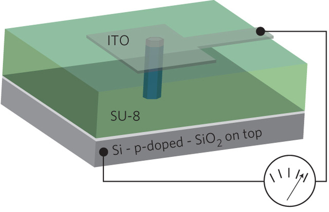
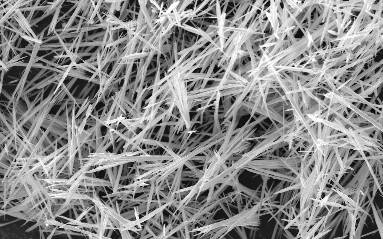
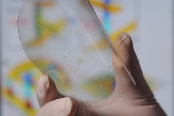 In essence, the skin is a transparent, flexible arrays that uses 8000 touch-sensitive transistors (aka. taxels) that emit electricity when agitated. Each of these comprises a bundle of some 1,500 zinc oxide nanowires, which connect to electrodes via a thin layer of gold, enabling the arrays to pick up on changes in pressure as low as 10 kilopascals, which is what human skin can detect.
Mimicking the sense of touch electronically has long been the dream researchers, and has been accomplished by measuring changes in resistance. But the team at Georgia Tech experimented with a different approach, measuring tiny polarization changes when piezoelectric materials such as zinc oxide are placed under mechanical stress. In these transistors, then, piezoelectric charges control the flow of current through the nanowires.
 In a recent news release, lead author Zhong Lin Wang of Georgia Tech’s School of Materials Science and Engineering said:
Any mechanical motion, such as the movement of arms or the fingers of a robot, could be translated to control signals. This could make artificial skin smarter and more like the human skin. It would allow the skin to feel activity on the surface.
This, when integrated to prosthetics or even robots, will allow the user to experience the sensation of touch when using their bionic limbs. But the range of possibilities extends beyond that. As Wang explained:
This is a fundamentally new technology that allows us to control electronic devices directly using mechanical agitation. This could be used in a broad range of areas, including robotics, MEMS, human-computer interfaces, and other areas that involve mechanical deformation.
 Not the first time that bionic limbs have come equipped with electrodes to enable sensation. In fact, the robotic hand designed by Silvestro Micera of the Ecole Polytechnique Federale de Lausanne in Switzerland seeks to do the same thing. Using electrodes that connect from the fingertips, palm and index finger to the wearer’s arm nerves, the device registers pressure and tension in order to help them better interact with their environment.
Building on these two efforts, it is easy to get a glimpse of what future prosthetic devices will look like. In all likelihood, they will be skin-colored and covered with a soft “dermal” layer that is studded with thousands of sensors. This way, the wearer will be able to register sensations – everything from pressure to changes in temperature and perhaps even injury – from every corner of their hand.
As usual, the technology may have military uses, since the Defense Advanced Research Projects Agency (DARPA) is involved. For that matter, so is the U.S. Air Force, the U.S. Department of Energy, the National Science Foundation, and the Knowledge Innovation Program of the Chinese Academy of Sciences are all funding it. So don’t be too surprised if bots wearing a convincing suit of artificial skin start popping up in your neighborhood!
 Source: news.cnet.com